Engineering Advanced Semiconductor Wafers

Advanced beyond-silicon semiconductor wafers enable state-of-the-art of semiconductor devices, but widespread adoption has been limited by technical and economic barriers.

K1 Semiconductor’s engineered composite wafers change the equation, unlocking adoption and redefining the possibilities for heterogeneous semiconductor systems.

The New Frontier of Semiconductor Chips

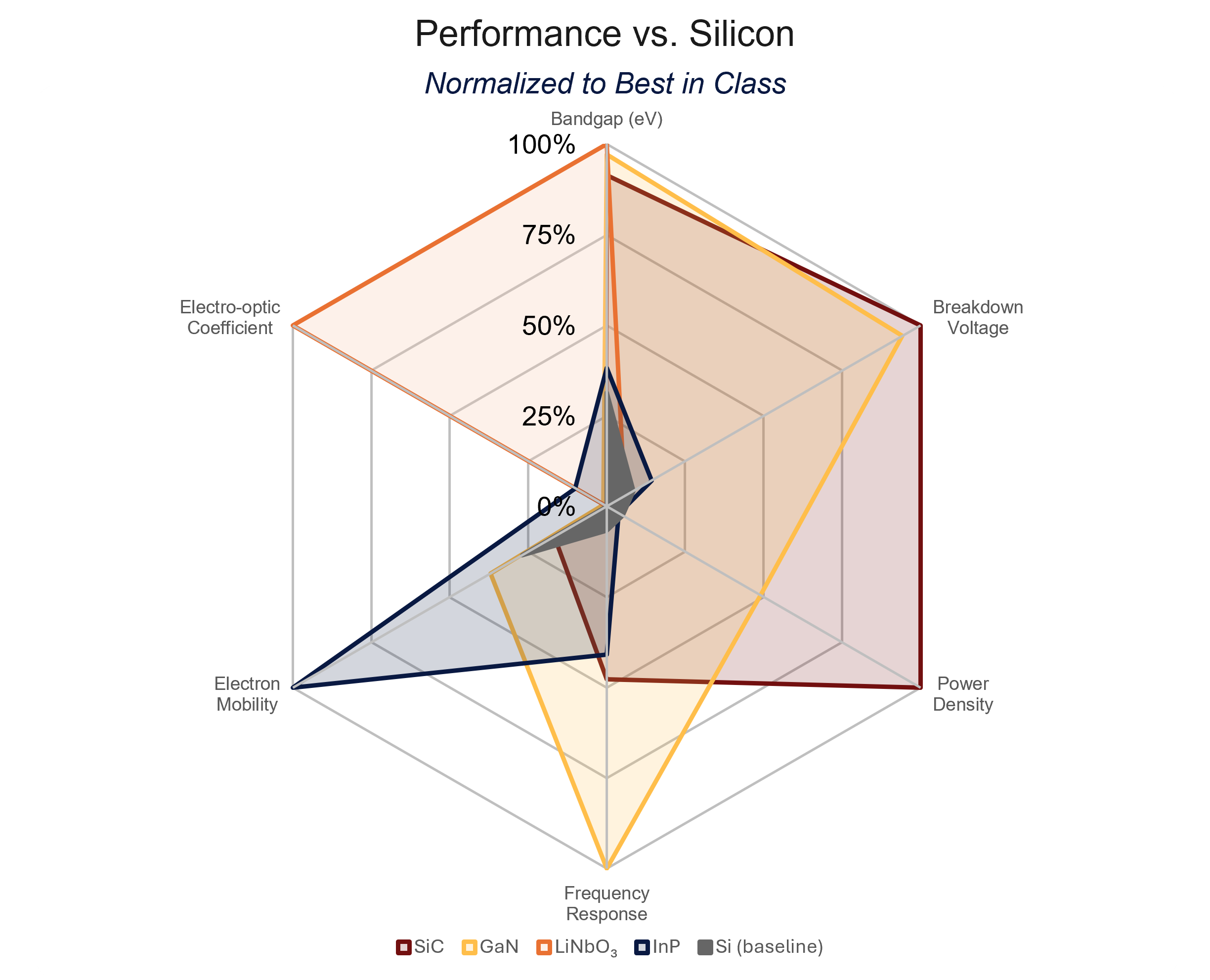
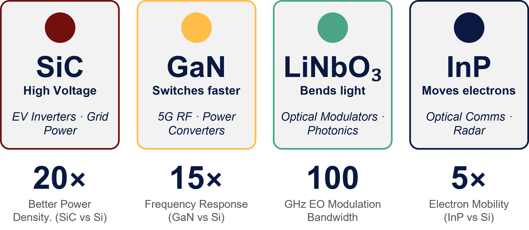
From AI data centers to quantum computing and telecommunications, global semiconductor innovation demands materials that can handle extreme voltage, heat, and/or freuqencies. Silicon is maxing out on all three. Next generation materials like silicon carbide, gallium nitride, lithium niobate, and indium phosphide are the solution, but efficiently integrating them into device architectures remains industry’s greatest bottleneck. Current techniques waste most of these expensive materials and were not built for heterogeneous systems of the future. K1 Semiconductor has found a way to bridge that gap.

Engineering the Perfect Composite Wafer

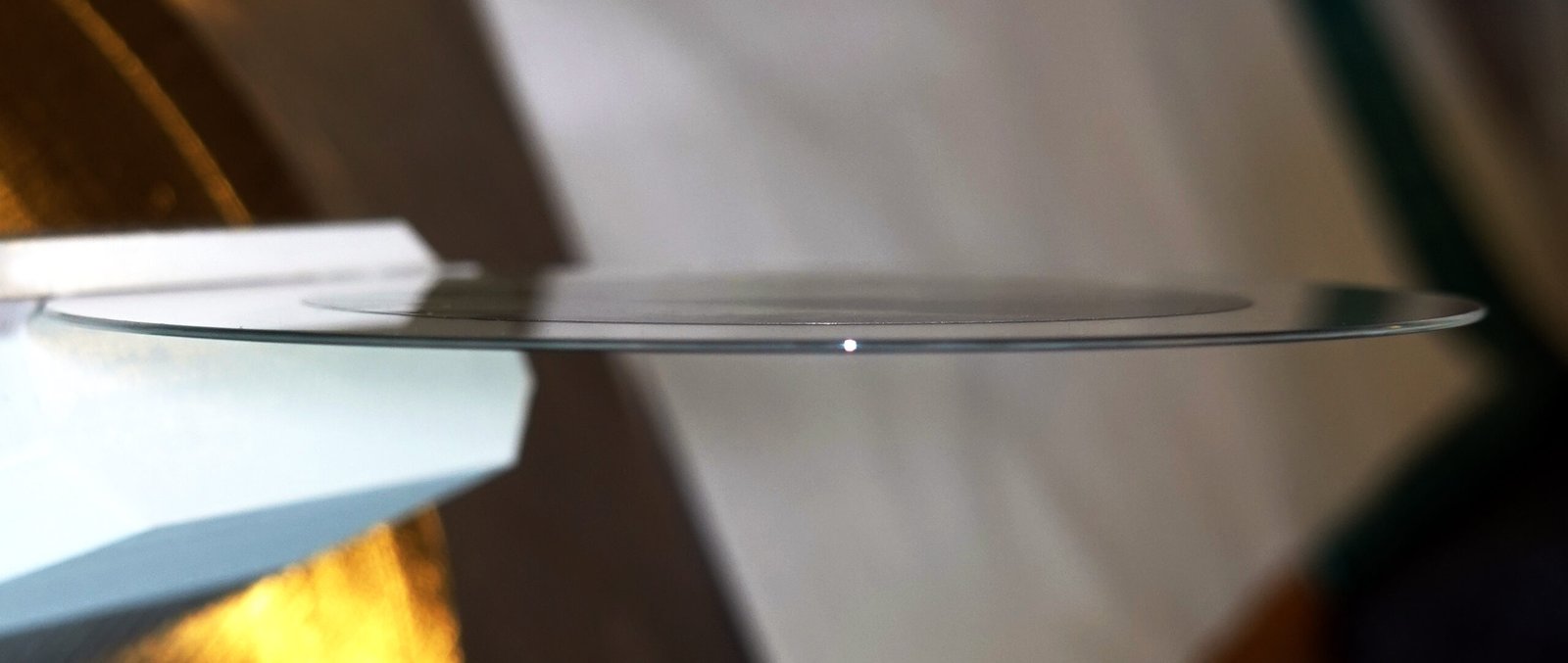
K1 Semiconductor provides the ideal, scalable solution through our innovative spalling technology. By depositing a highly stressed layer to carefully propagate a subsurface crack, we deterministically release a flawless active layer from the parent wafer. By bonding this pristine layer to an engineered handle wafer, we deliver uncompromised bulk-quality performance at a fraction of the traditional material cost.

K1’s Breakthrough technology

K1’s wafer-splitting (“spalling”) platform technology produces thin layers that can enable engineered composite wafers delivering generational performance gains.

The K1 Team

K1 is led by a multidisciplinary team of scientists, engineers, and business operators — backed by world-class advisors experienced in semiconductor manufacturing and deep-tech commercialization.